Business Areas

Connected Insight delivers integrated vision technology
optimized for diverse industries.

PCB

Copper Plate & Copper Film Surface Inspection

Captures images at high speed with 7–14μm resolution and processes large-area imagery to acquire uniform images.
Rule-based and AI inspection run simultaneously to improve detection performance and handle large-volume images effectively.
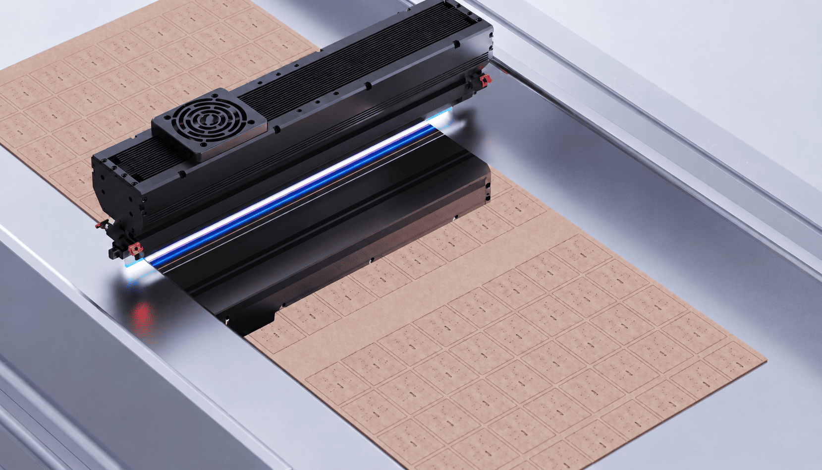
Copper plate and copper film surface inspection image 1
[Lead Frame appearance inspection]
Copper plate and copper film surface inspection image 2
[Precision results screen of the defect tracking system]

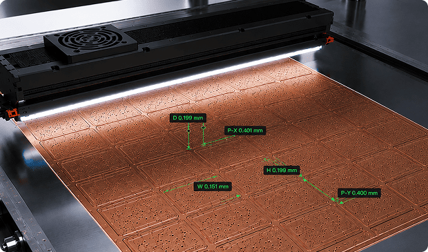
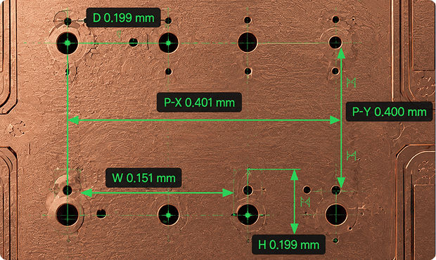
Copper Plate Pattern Hole and Spacing Inspection

Precisely measures copper plate hole and pattern spacing dimensions with 7μm high-resolution images.

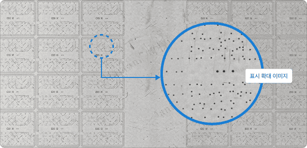
Copper plate pattern hole and spacing inspection image 1
[Real-time scan of hole interior status on the PCB board]
Copper plate pattern hole and spacing inspection image 2
[Inspection results detecting hole interior defects with magnified area analysis]