
Solution
Connected Insight solutions use AI machine vision and deep learning
to deliver quality inspection and automation across manufacturing processes.
Large-area Inspection Solution

Large-area Inspection Solution Applied Technologies
-
CIS line-scan cameras inspect wide areas from 165mm to 1,600mm+ in a single pass
-
80,000 lines per second with stable image quality at scan speeds up to 1,000mm/s
-
Optimized optics minimize illumination variation for high-quality image capture
-
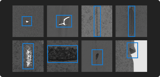
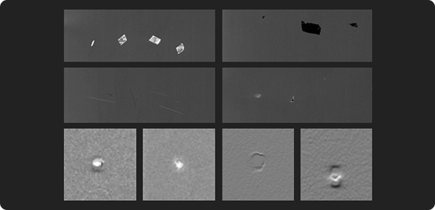
AI inspection algorithms automatically classify defect types to improve detection accuracy
Large-area Inspection Solution Applications
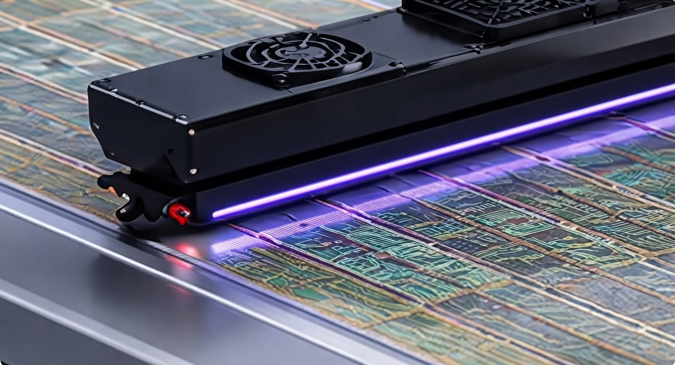
CIS line-scan camera-based large-area inspection is applied across diverse industries that require high-speed, high-resolution inspection of wide areas.
It enables real-time inspection of surface defects and quality for large-area materials and products including display, secondary battery, solar, film/coating, semiconductor, and more.
Connected Insight minimizes illumination variation and image quality degradation that can occur in large-area inspection through wide FOV, high-speed line acquisition technology, and optimized optical and lighting systems, delivering stable inspection performance.
-
Wide Scan Width 16mm~1600mm+ Single wide pass scan
-
Image Uniformity 80,000 lines/sec Ultra-fast acquisition
-
System Configuration Up to 1,000mm/s Stable image quality
-
High-speed Inspection Optimized optical system Minimal variation


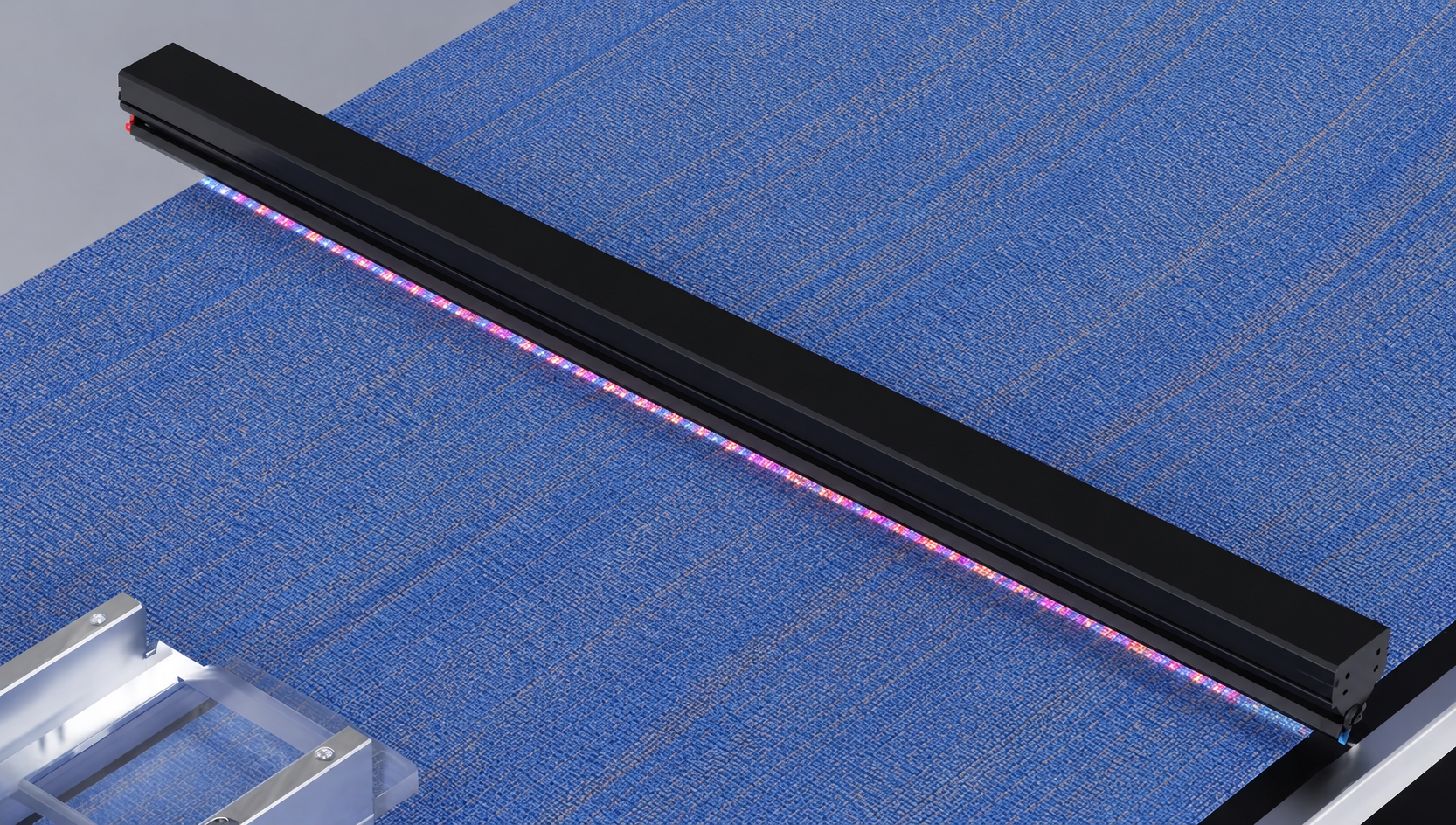
Fabric Surface Inspection

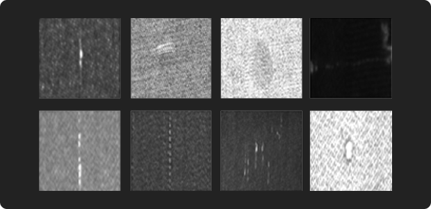
Battery Separator Surface Inspection
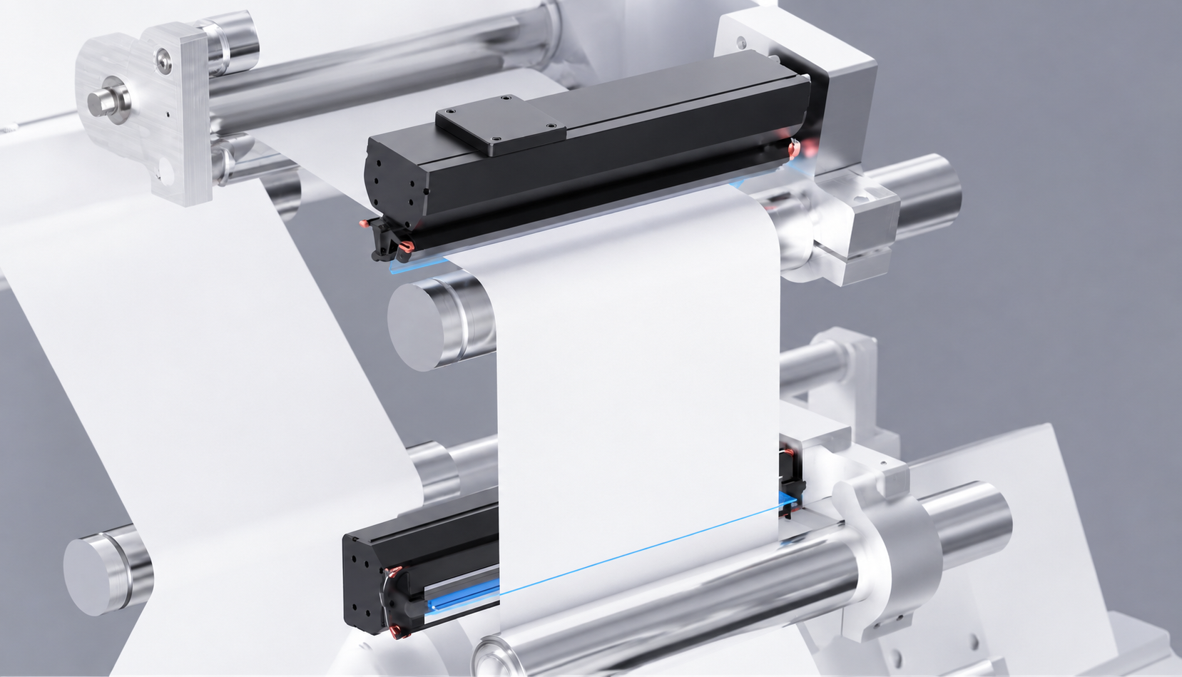
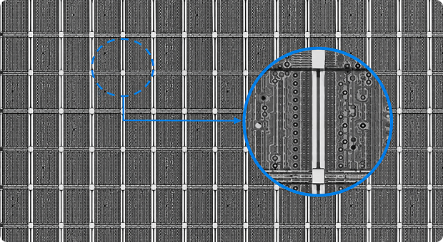
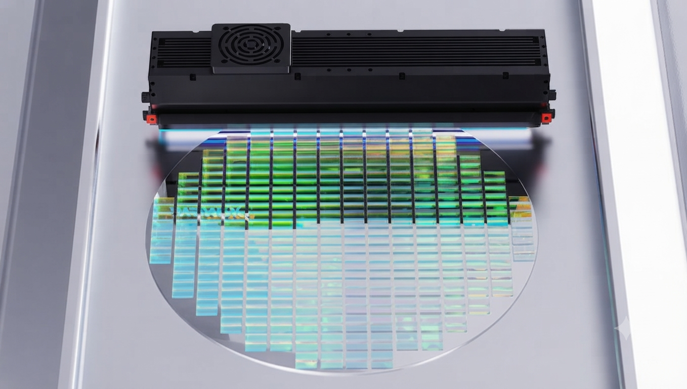
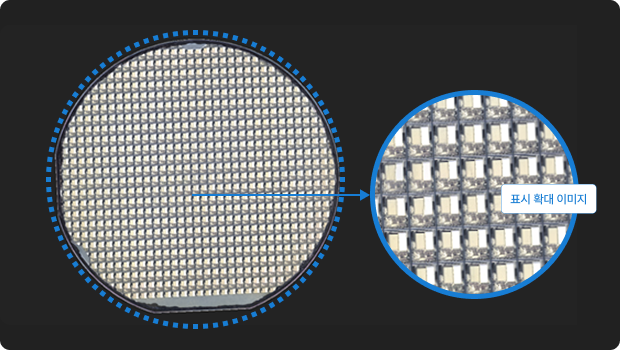
Semiconductor Wafer Surface Inspection
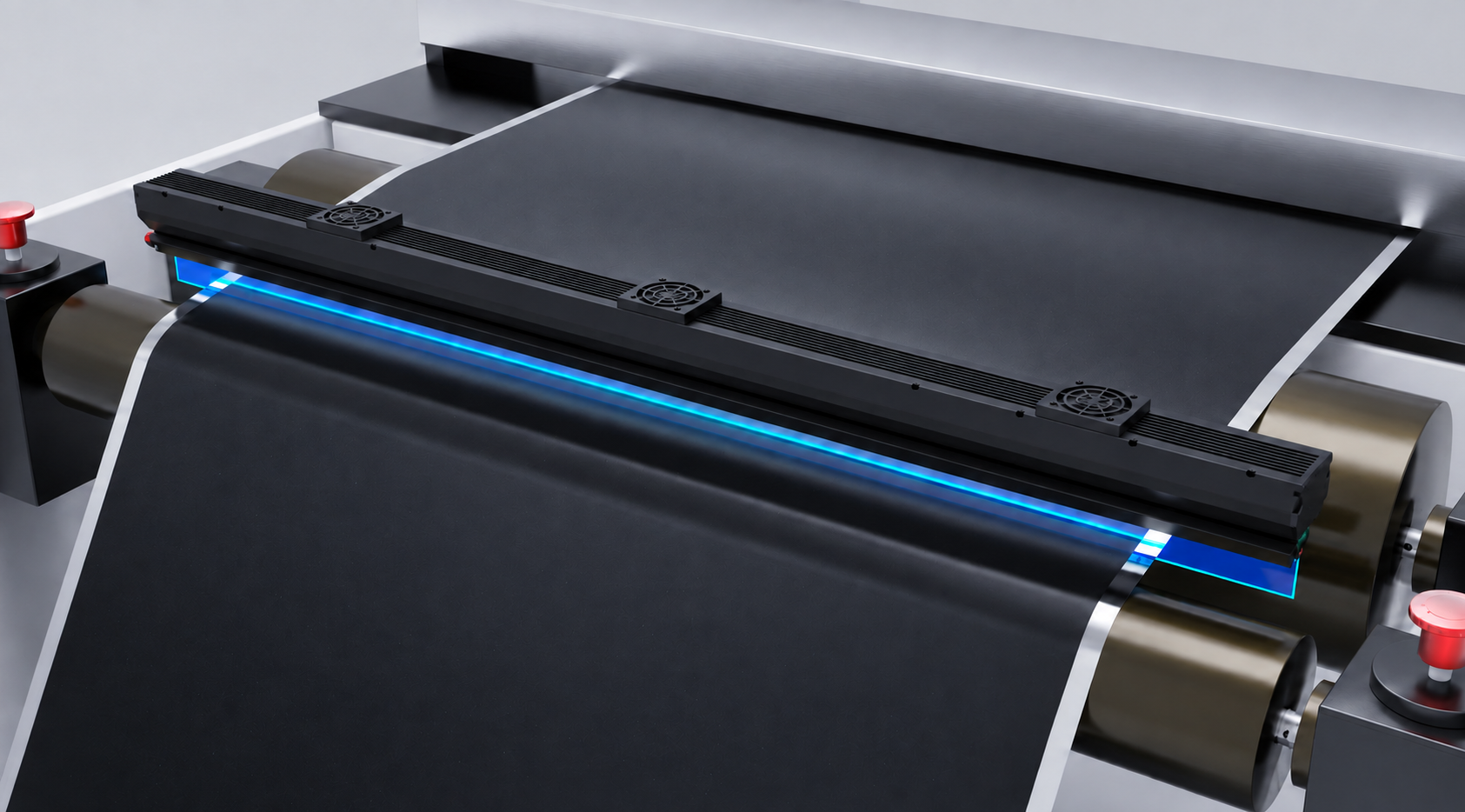
Lithium Battery Electrode Defect Inspection
CIS solutions support coating, indentation, and dent inspection for major battery manufacturers worldwide. A 1550mm wide camera inspects with no missed areas.
It helps maintain core process yield at 99% and significantly reduce overall operating costs.
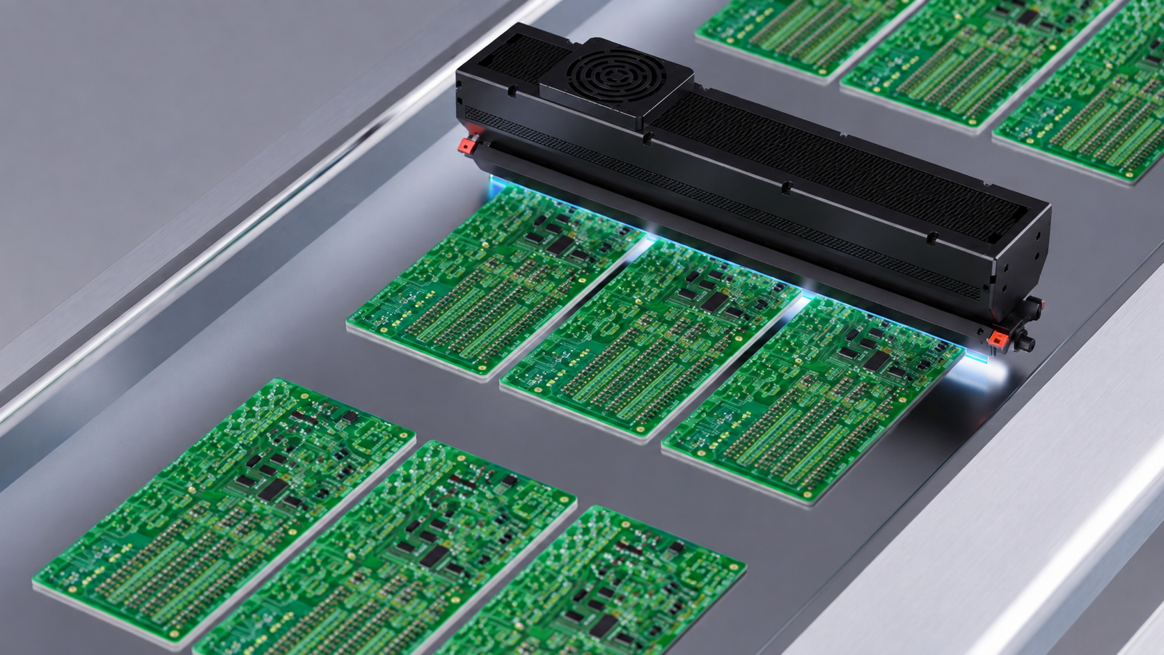
PCB Hole and Surface Inspection
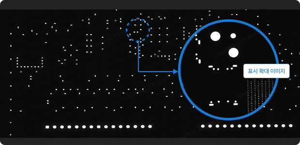
Display Cell Panel Surface Inspection