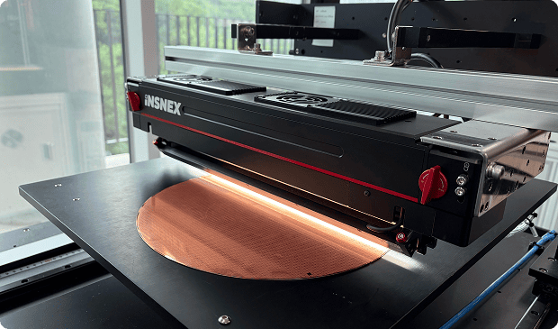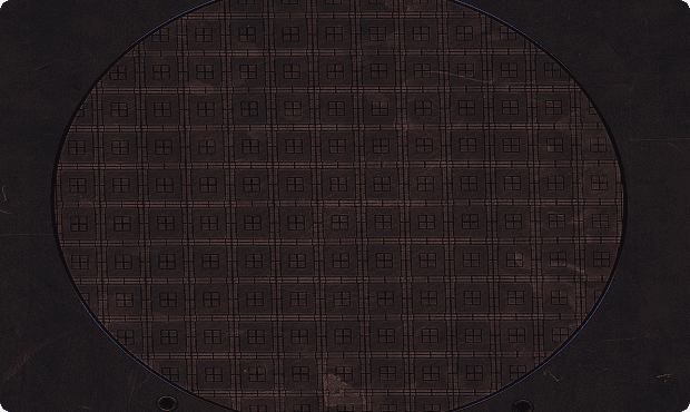


Wafer Edge Crack Inspection System

Magnifies and measures only the wafer edge, effectively detecting chipping while the wafer rotates.
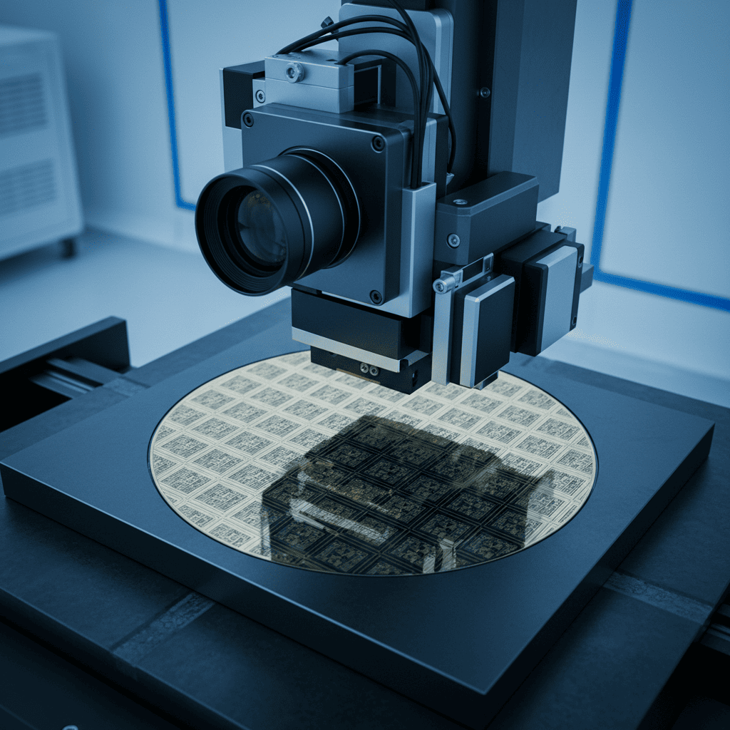
Scene of non-contact inspection of wafer surface and micro-pattern condition

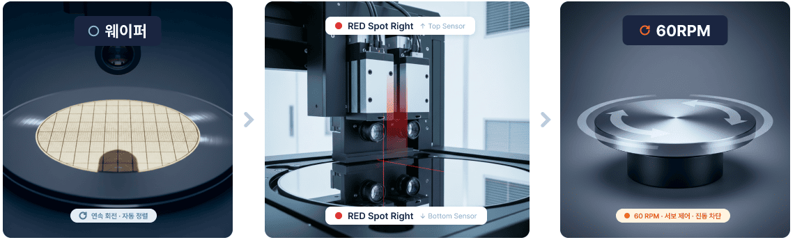
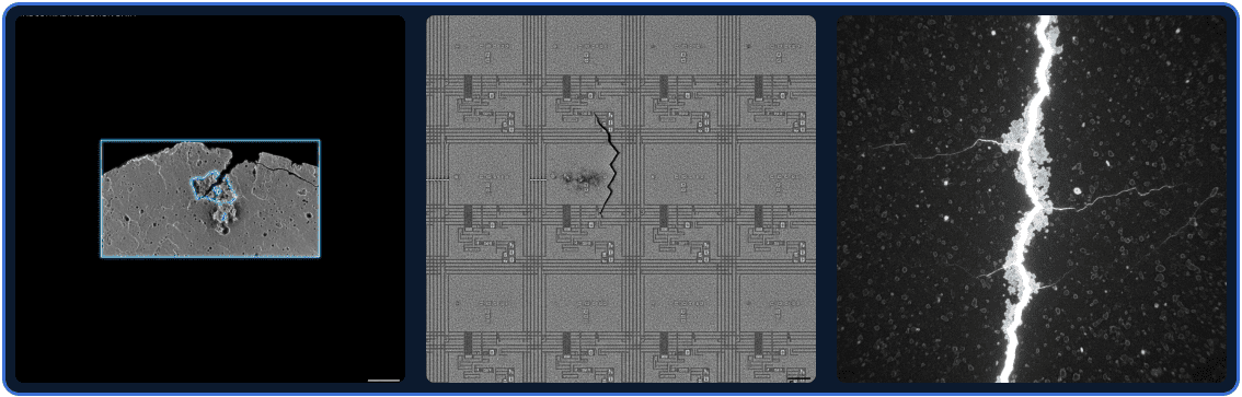
Actual captured data with precise detection of edge micro-defects and pattern condition
[Operating principle and inspection process of the post-process semiconductor surface AOI (automatic optical inspection) system]